1/ Overview
Electronic components are the fundamental building blocks of circuits and systems that process, control, convert, sense, store, or transmit electrical energy and information. A complete technical treatment covers component classification, electrical and thermal behaviors, packaging and mounting, PCB integration, modelling and simulation, reliability and failure modes, test and verification methods, supply-chain considerations, and practical selection and design rules for robust products.
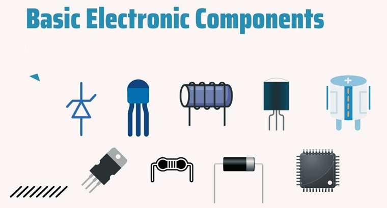
2/ Classification and roles
2.1/ Passive components
- Resistors: fixed, variable, thermistors (NTC/PTC), shunt/current-sense resistors; key specs: resistance, tolerance, power rating, temperature coefficient, noise, pulse-withstand.
- Capacitors: ceramic (MLCC), film, electrolytic (wet/dry), tantalum, supercapacitors; key specs: capacitance, voltage rating, ESR, ESL, temperature coefficient (dielectric class), ripple current, lifetime (electrolytics).
- Inductors and transformers: power inductors, chokes, RF inductors, coupled inductors; specs: inductance, DC resistance, saturation current, Q-factor, self-resonant frequency.
2.2/ Active components
- Diodes: rectifier, Schottky, Zener, TVS, PIN, photodiodes, LEDs; specs: Vf, reverse leakage, reverse breakdown, recovery time, power dissipation.
- Transistors: BJTs, MOSFETs (enhancement P/N), JFETs, IGBTs; specs: Vce/Vds rating, current rating, gain/hFE, Rds(on), threshold Vth, gate charge Qg, safe operating area (SOA), switching times.
- Integrated circuits (ICs): linear (op-amps, references, LDOs), switching power converters (buck/boost/SEPIC), mixed-signal (ADC/DAC, regulators with telemetry), digital logic families, microcontrollers, FPGAs, SoCs.
- Sensors and actuators: temperature, pressure, inertial, optical, magnetic sensors; stepper/servo drivers and multiplexers.
2.3/ Electromechanical and interconnects
Connectors, relays (electromechanical and solid-state), switches, potentiometers, sockets, heatsinks, fans.
3/ Electrical, thermal and dynamic characteristics
3.1/ Key electrical parameters
- DC parameters: resistance, capacitance, inductance, breakdown voltage, leakage, bias dependence.
- AC parameters: impedance vs frequency, ESR/ESL for capacitors, S-parameters for RF components, gain-bandwidth and slew for amplifiers.
- Nonlinear behavior: diode I - V exponential, MOSFET subthreshold, transistor early effect, varistor/VDR characteristics.
3.2/ Thermal behavior
- Power dissipation and thermal resistance chain: Pd → junction → case → board → ambient. Use θJA, θJC and thermal vias/heatsinking to manage junction temperature.
- Derating rules: derate voltage, current and power with temperature and altitude; follow datasheet derating curves.
- Thermal transients: calculate time constants for heating and cooling for power cycling and thermal shock analysis.
3.3/ Switching and dynamic limits
- Parasitics matter: trace inductance, package capacitance, device capacitances (Cgs, Cgd, Cds), recovery charge Qrr in diodes.
- EMC implications: di/dt and dv/dt cause emissions and ringing; snubbers, RC dampers, ferrites address these.
4/ Packages, mounting and PCB integration
4.1/ Package types and trade-offs
- Through-hole: robust mechanical retention, easier rework, poorer area efficiency.
- SMD: SOT, SOIC, QFN, TSSOP, QFP, BGA; benefits: smaller parasitics, high density, automated assembly; challenges: thermal pad design, rework, inspection (BGA X-ray).
- Power packages and thermal pads: packages with exposed pads require solderable thermal vias and copper pour for heat spreading.
4.2/ PCB layout best practices
- Bypass and decoupling: place MLCCs close to supply pins; combine values (e.g., 0.1µF + 1µF + electrolytic) to cover frequency bands.
- Grounding: single-point vs multipoint considerations; use solid ground planes and controlled impedance for high-speed lines.
- Power traces and copper pours sized for current; use thermal reliefs for large copper areas where needed.
- High-speed signal integrity: controlled impedance traces, matched lengths for differential pairs, avoid stubs, include proper terminations.
- Thermal relief: thermal vias under power IC pads, via stitching for heat spread.
5/ Modelling, simulation and characterization
5.1/ SPICE and behavioural models
- Use manufacturer SPICE models for MOSFETs, diodes and complex ICs; verify model validity across temperature and bias conditions.
- Behavioral models (Verilog-A, VHDL-AMS) for system-level mixed-signal simulation.
5.2/ Thermal and electrothermal simulation
- Use finite-element or lumped thermal network models to size heatsinks and heat-spreading copper.
- Co-simulate electrical switching events and thermal response for accurate switching-loss and temperature rise predictions.
5.3/ RF and EMC analysis
- S-parameter measurements and simulations for RF components and matching networks.
- Time-domain reflectometry (TDR) for impedance discontinuities on transmission lines.
6/ Reliability, failure modes and mitigation
6.1/ Common failure modes
- Electrolytic capacitor drying or ESR increase; ceramic MLCC cracking under mechanical stress or DC bias capacitance drop.
- Solder joint fatigue due to thermal cycling; pad lift from overheating.
- Gate oxide damage or latch-up in MOSFETs and CMOS; hot-carrier degradation in transistors.
- ESD and overvoltage transients damaging semiconductors.
6.2/ Reliability engineering practices
- Design margining: select components with voltage/current ratings higher than operating extremes.
- Thermal management: keep junction temperatures within safe limits; add airflow, heatsinks, thermal interface materials.
- Stress screening: burn-in, temperature cycling, humidity and vibration tests to detect infant mortality.
- Use FMEA/FTA and MTBF modeling where appropriate; track field returns and institute corrective actions.
6.3/ ESD and surge protection
- TVS diodes, series resistors, common-mode chokes, input filtering and proper grounding.
- PCB layout to separate sensitive analog/digital domains and minimize loop area.
7/ Testing, validation and qualification
7.1/ Component-level verification
- LCR meters, curve tracers, semiconductor parameter analyzers, and S-parameter network analyzers.
- X-ray inspection for BGA voids and solder quality.
7.2/ Board-level testing
- In-circuit test (ICT) and flying probe for net connectivity and passive component presence/values.
- Boundary-scan (JTAG) for digital interconnects, especially for BGAs.
- Functional test (FCT) with instrumented fixtures, test vectors, and power sequencing checks.
7.3/ Environmental qualification
- Thermal cycling, thermal shock, humidity (HAST), salt spray for corrosion-prone environments, vibration and shock.
- EMC compliance testing for radiated and conducted emissions and immunity.
8/ Selection, sourcing and obsolescence management
8.1/ Selection process
- Specify electrical, mechanical and environmental requirements first; then filter parts by datasheet margins and lifecycle status.
- Evaluate alternate suppliers and second-source qualified parts; consider long-lead or custom components early.
8.2/ Supply-chain practices
- Maintain approved vendor list (AVL) and authorized distributor relationships to avoid counterfeit parts.
- Keep alternate BOMs and footprint compatibilities; plan for end-of-life (EOL) and last-time-buy windows.
8.3/ Cost vs performance trade-offs
- Optimize BOM by choosing integrated solutions where board area and assembly cost outweigh marginal per-part savings.
- Use standard footprints to allow cross-qualification.
9/ Practical design rules and checklists
- Power rails: place decoupling capacitors within 2 - 5 mm of IC power pins; add bulk capacitance near regulators.
- MOSFET selection: choose Vds margin of at least 1.5 - 2x operating voltage; minimize Rds(on) for conduction loss but assess Qg for gate-drive losses.
- Capacitor selection: use MLCC for high-frequency decoupling; provide electrolytic or polymer bulk for low-frequency energy storage.
- Thermal design: ensure θJA and θJC are compatible with allowable junction rise; provide thermal vias and copper area under power ICs.
- Layout review: run signal-integrity and power-integrity simulations; check for long return loops, 90-degree bends, and inadequate spacing for high voltages.
- EMC: route noisy traces away from antennas and sensitive analog inputs; use common-mode chokes and ferrite beads on I/O lines.
10/ Conclusion
A complete, technical mastery of electronic components combines deep understanding of device physics and datasheet parameters, disciplined PCB and thermal design, rigorous modelling and validation, and proactive reliability and supply-chain management. Applying these principles allows engineers to design compact, efficient and reliable electronic systems across consumer, industrial, automotive and aerospace domains.
By now you must have understood about electronic components. We, QTE Technologies provide thousands of different types of electronic components from world famous brands.
QTE Technologies is a proud global MRO provider, serving customers in over 180 countries and always striving to ensure a complete and satisfying customer experience. Established in 2010, we offer over 1 million products across every industry and technology. Additionally, you can reach us anytime via 24×7 chat support, phone, WhatsApp or email. Discover what our valued customers have to say about our services on our dedicated review page.
Author of the article: Editorial Board of QTE Technologies (with a solid background in both engineering and creativity - accumulated over 15 years of experience).