1/ Overview and concepts
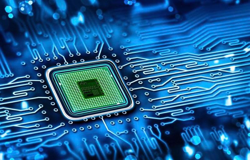
A semiconductor is a material whose electrical resistance lies between that of a conductor (metal) and that of an insulator, with the ability to adjust its conductivity based on temperature, light or impurity concentration. This is the basis for most electronic components from transistors, microcircuits to LEDs and sensors.
2/ Applications of semiconductors in major fields
2.1/ Information technology
Semiconductors are the basis of microprocessors, memories and sensors in all digital systems from central servers to smartphones and data centers. They are responsible for processing, storing and transmitting information at high speed and efficiency, and play a core role in all modern electronic devices.
2.2/ Consumer electronics
Most household electronic devices such as smart TVs, game consoles, smart watches and smart home devices use semiconductor components. These components control interfaces, process video and audio signals, and connect to the Internet, contributing to a seamless and rich user experience.
2.3/ Automotive Industry
In modern automobiles, semiconductors are integrated into engine control systems, electric drives, autonomous driving assistance systems, and safety sensors. They are used to measure tire pressure, distance, detect obstacles, and manage energy, improving vehicle safety and fuel efficiency.
2.4/ Renewable Energy
Photovoltaic cells use semiconductors to convert sunlight into electricity. Crystalline silicon, thin-film, and perovskite technologies are developing rapidly, reducing manufacturing costs and increasing solar energy conversion efficiency.
2.5/ Internet of Things (IoT) and sensors
Semiconductors enable the manufacture of small-sized, low-power sensors for temperature, light, humidity, pressure and other environmental parameters. They are integrated in surveillance cameras, smart agricultural measuring devices, smart cities and the medical industry such as heart rate sensors or blood oxygen saturation sensors.
2.6/ Optoelectronic and microwave devices
III-V semiconductors (GaAs, InP) are used in laser diodes, photodetectors and microwave components for telecommunications, radar and 5G/6G networks. Wide-bandgap materials (SiC, GaN) are also used in high-power and specialized radio frequency devices, improving performance and durability in harsh environments.
3/ 2D Materials in Semiconductors
3.1/ Concept and History of Discovery
2D materials are substances that are only one or a few atoms thick, exhibiting unique electrical, optical and mechanical properties compared to traditional 3D materials. Graphene, a single-atom layer of carbon “extracted” from graphite by Andre Geim and Konstantin Novoselov in 2004, was the first 2D material to be recognized and won the 2010 Nobel Prize in Physics for its outstanding electrical conductivity and mechanical strength.
3.2/ Important 2D materials
- Graphene: extremely high electrical conductivity, electrons move at speeds up to 1/300 the speed of light, good thermal conductivity and a surface area of up to 2% that absorbs visible light.
- TMDs (MoS₂, WS₂): disulfide-type metal-metal junctions with energy gaps suitable for transistors and photodetectors.
- Phosphorene: from phosphorus, with bandwidth varying according to the number of layers, suitable for flexible applications.
- Silicene: 2D analog of silicon, promising direct integration with existing CMOS.
- Borophene, vonene and single-layer gold: discovered in 2015 and 2024 respectively, opening the door for diverse 2D materials with special mechanical and electrical properties.
3.3/ Applications in semiconductor components
2D materials are being studied to replace or supplement silicon in many components thanks to advantages in size, performance and energy consumption:
- Ohmic contacts: MoSi₂N₄ and WSi₂N₄ create easy contacts with titanium, scandium, nickel, reducing Schottky barrier and energy loss when connecting metal-semiconductor.
- Transistors and integrated circuits: thin 2D channels reduce short-channel penetration and low power consumption.
- Sensors and opto devices: single-atom layers increase photoelectric and electrochemical sensitivity, applied in photodetectors and ultra-thin LEDs.
Sources from the Singapore University of Technology and Design show that a generation of low-power electronic devices, with a miniaturization of millions of transistors that can be packed into a chip the size of a fingernail, is becoming a reality thanks to 2D materials.
3.4/ Challenges and development trends
- Metal bonding - 2D: Fermi level pinning makes it difficult to control electrical contact, research teams are looking for new buffer materials or contact techniques to create the desired high and low barriers.
- Mass production capability: many 2D materials still have difficulty in manufacturing uniformly and purely on large areas.
- Integration with CMOS processes: thermal, chemical compatibility and long-term reliability are required before commercialization.
4/ Why are 2D materials important in modern technology?
4.1/ Superior electrical and thermal performance
2D materials such as graphene, TMDs (MoS₂, WS₂) possess a very large surface area compared to volume, allowing for excellent electrical conductivity and more efficient heat dissipation than traditional semiconductor layers. Only one or a few atoms thick, they almost completely eliminate uneven electron collisions, thereby reducing energy loss and increasing signal transmission speed.
4.2/ Optimized size and energy consumption
With a thickness of only a few ångströms, 2D channels can be hundreds of thousands of times thinner than a human hair, significantly reducing short-channel effects when shrinking transistor size. This paves the way for packaging millions of transistors in a chip as small as a fingernail, while lowering operating voltage and energy consumption.
4.3/ Mechanical and optical flexibility
Extremely thin and flexible 2D films enable the creation of electronic components, sensors and foldable displays without destroying the structure. The light absorption capacity of TMDs or phosphorene layers is also very high, opening up applications in photodetectors, ultra-thin LEDs and solar cells integrated directly into flexible materials, fabrics or glass.
4.4/ High functional customization
By choosing the elements and number of layers, researchers can directly tune the energy gap (bandgap), electron kinetics and surface properties. For example, from graphene (near-zero bandgap) to MoS₂ (~1.8 eV bandgap), 2D materials allow the design of components from ultra-fast to ultra-optical sensitivity, or the integration of multiple functions (multi-channel, multi-sensor) on the same thin platform.
4.5/ Breakthrough applications in all fields
- Microelectronics: pico-watt transistors, next-generation logic circuits.
- Healthcare: skin-mounted biosensors, ultra-sensitive measurement of biomarker concentrations, electrochemistry.
- Energy: perovskite-2D solar cells, ultra-thin storage integrated into material structures.
- Telecommunications: RF/GaN-2D components for 5G/6G networks and high-resolution radar.
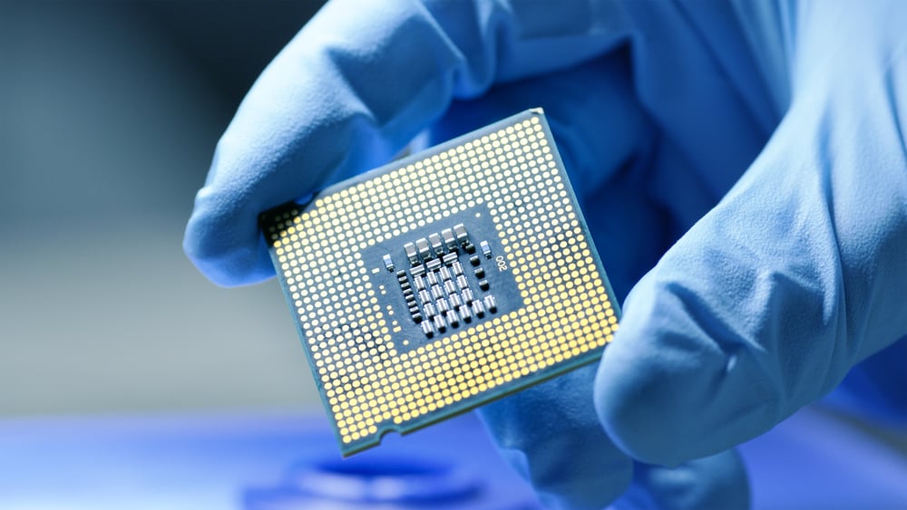
QTE Technologies is currently distributing semiconductors of many famous brands in the world.
We are proud to be a global MRO supplier, serving customers in more than 180 countries and always striving to ensure customers have a complete and satisfied experience. We were founded in 2010, supplying more than 1 million products for all industries and science and technology. Alternatively, you can reach us anytime via 24×7 chat support, phone, WhatsApp or email. Discover what our valued customers have to say about our services on our dedicated review page.
Author: Editorial team of QTE Technologies (with a strong background in both engineering and creativity - over 15 years of experience).